Thermal Reliability Challenges in Co-Packaged Photonic Systems
Integrating optical waveguides directly into 2.5D/3D multi-die packages solves bandwidth bottlenecks, but co-locating high-power GPU/ASIC compute dies creates intense 100–300 W/cm² thermal fluxes that threaten optical link integrity.
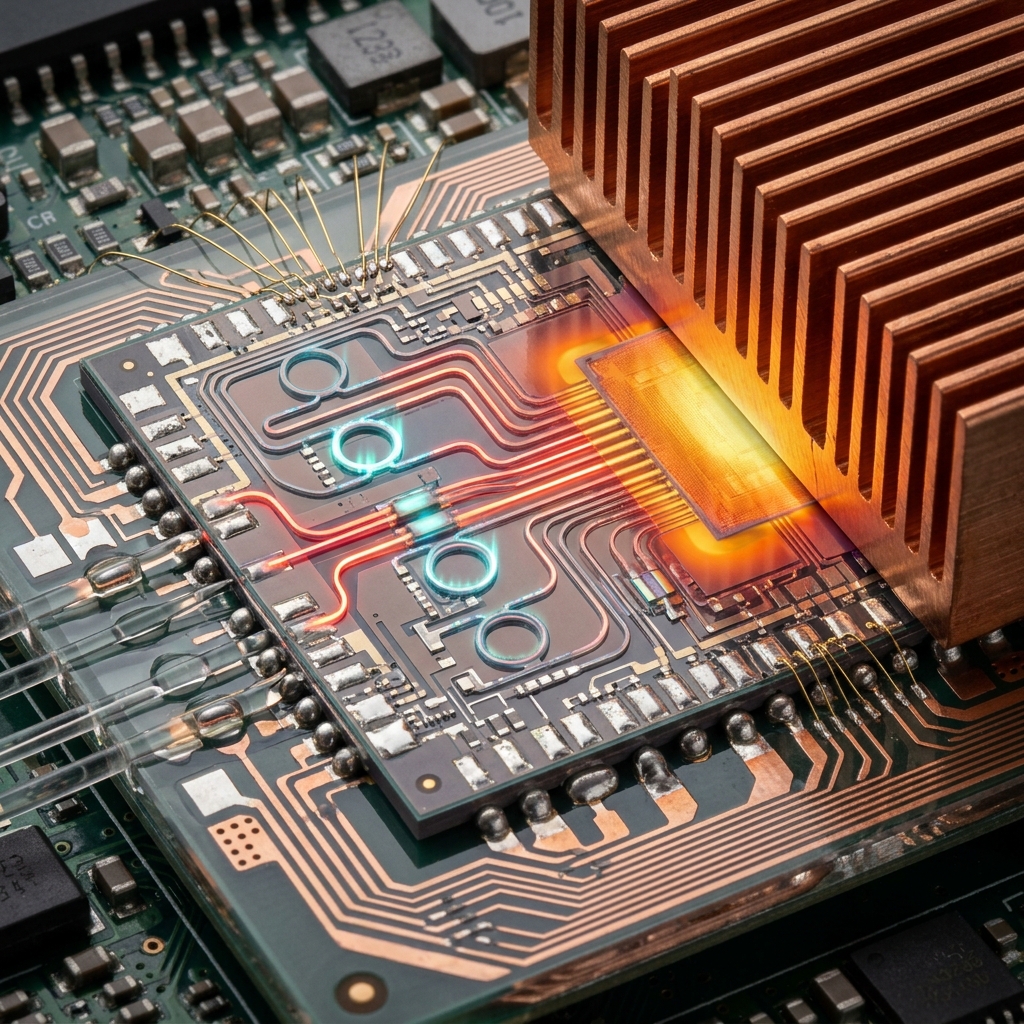
Architectural Overview
Integrating optical waveguides directly into multi-die packages (such as Co-Packaged Optics (CPO), 2.5D/3D ICs, and System-in-Package architectures) resolves electrical interconnect power and bandwidth bottlenecks. However, co-locating high-power compute dies (GPUs, Switch ASICs) with optical engines creates intense local thermal fluxes.
Under severe thermal dissipation (often exceeding 100–300 W/cm² locally), optical waveguides face critical thermo-optic, mechanical, and material reliability challenges that require specialized athermal architectures, thermal tuning, and packaging co-design.
1. Key Degradation Mechanisms Under High Thermal Flux
Thermo-Optic Phase Drift & Resonant Frequency Shifts
The thermo-optic effect (dn/dT) in silicon (approx. 1.8 × 10⁻⁴ K⁻¹) creates local temperature gradients that alter the refractive index of the waveguide core relative to its cladding. Consequently, Mach-Zehnder Interferometers (MZIs) and microring resonators (MRRs) experience significant resonance wavelength drift (~0.08 to 0.1 nm/°C). High spatial temperature gradients across multi-die packages lead to severe channel crosstalk and insertion loss in Dense Wavelength Division Multiplexing (DWDM) links.
Thermo-Mechanical Stress & Coupling Misalignment
A mismatch in the Coefficient of Thermal Expansion (CTE) between silicon (2.6 × 10⁻⁶/K), polymer cladding (30–60 × 10⁻⁶/K), organic substrates, and metallic solder bumps generates significant shear stress during thermal cycles. Because edge couplers and grating couplers rely on sub-micron alignment tolerances, thermal expansion warping (warpage) induces axial and lateral displacement. This leads to coupling power loss (>1–3 dB) or catastrophic micro-cracking at fiber/waveguide interfaces.
Material Degradation & Outgassing
Polymer waveguides/claddings—including polyimide, acrylate, or epoxy-based materials—degrade at sustained elevated temperatures (>105–125°C). This results in thermo-oxidative yellowing, increased propagation loss (dB/cm), and altered mode confinement. Additionally, cyclic thermal flux causes stress concentration along the waveguide-cladding and waveguide-substrate interfaces, leading to interfacial delamination and optical scattering, which can result in complete link failure.
2. Failure Modes and Impact Matrix
| Reliability Hazard | Physical Origin | Primary Impact on Link | Mitigation Strategy |
|---|---|---|---|
| Resonance Wavelength Drift | Thermo-optic shift (dn/dT) in Si/SiN | Signal attenuation, crosstalk in WDM | Micro-heaters, closed-loop thermal tuning, athermal waveguides |
| Coupling Misalignment | CTE mismatch & package warpage | High insertion loss, optical power drop (>1–3 dB) | Passive compliance structures, low-CTE interposers (e.g., Glass/Si) |
| Interfacial Delamination | Thermal cycling stress (>40 MPa) | Optical scattering, complete link failure | Advanced adhesion promoters, stress-relieved buffer layers |
| Cladding Discoloration/Loss | High-temp polymer oxidation (>105°C) | Increased linear attenuation (dB/cm) | High-Tg inorganic claddings (SiO₂, Si₃N₄) |
3. Engineering Strategies to Enhance Reliability
Athermal Waveguide Architectures
- Overlay Engineering: Overlaying silicon waveguides with materials having a negative thermo-optic coefficient (e.g., specific polymers or titanium dioxide) to offset silicon's positive +dn/dT.
- Material Selection: Utilizing Silicon Nitride (Si₃N₄) waveguides, which exhibit a significantly lower thermo-optic coefficient (≈ 2.4 × 10⁻⁵ K⁻¹) and higher optical power handling limits.
Active Thermal Management & Tuning
- Integrated Micro-Heaters: Titanium/Platinum resistive micro-heaters localized directly over resonant structures dynamically stabilize waveguide temperatures against ASIC workload fluctuations.
- On-Chip Cooling: Micro-TECs or embedded microchannel liquid cooling integrated into the package interposer extract high localized heat fluxes before reaching sensitive optical paths.
Substrate & Packaging Material Optimization
- Glass Interposers (TGV): Glass provides superior mechanical stability, lower RF losses, and CTE matching closer to optical fibers, dramatically reducing coupling drift under thermal cycling.
- Photonic Wire Bonding (PWB): Flexible 3D polymer optical connections adapt to micro-displacements and thermo-mechanical stress significantly better than rigid fiber arrays.